Wiring
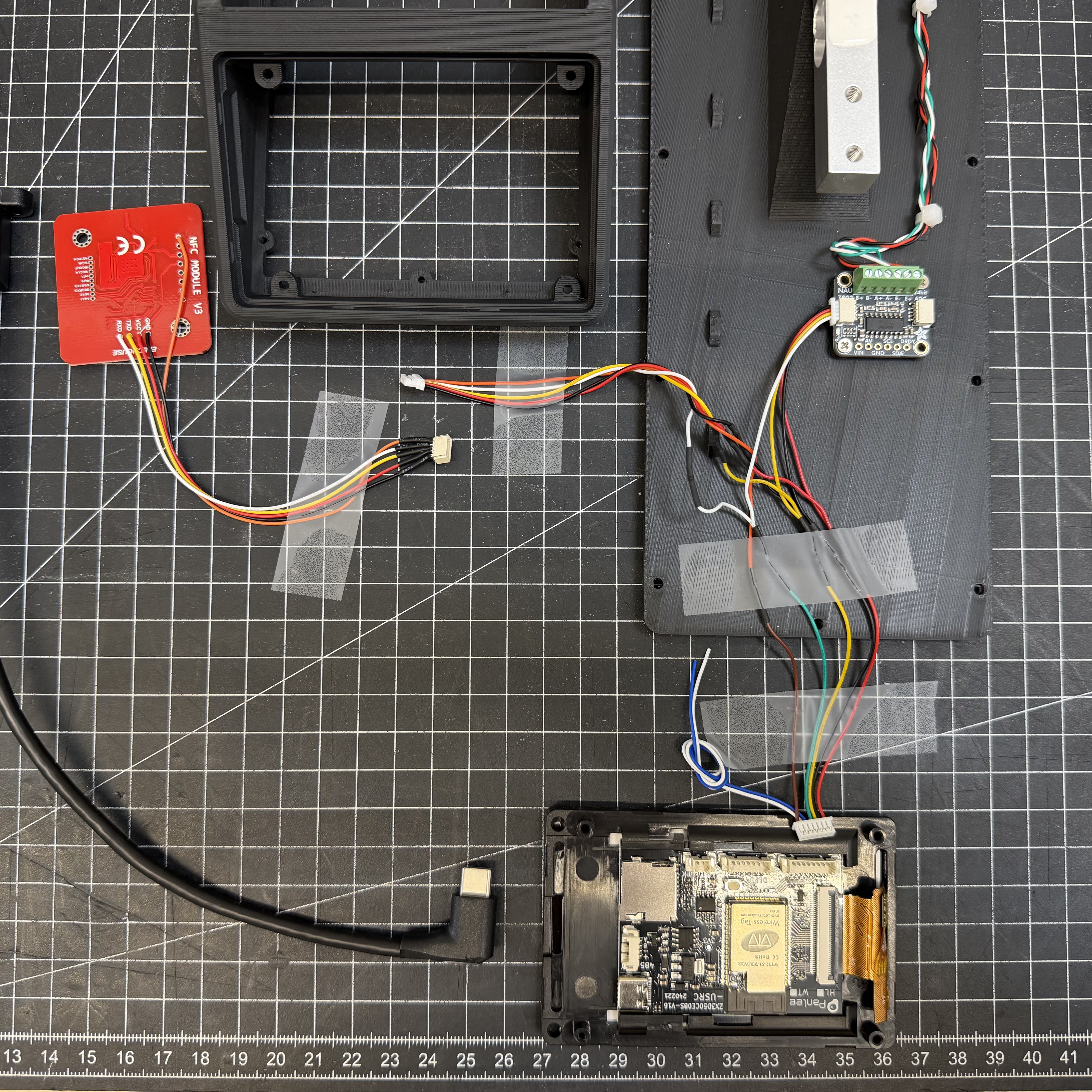
All components connect to the I/O connector on the WT32-SC01 Plus using the included 7-pin cable. The I/O socket has 8 pins - plug the 7-pin cable in flush to the left.
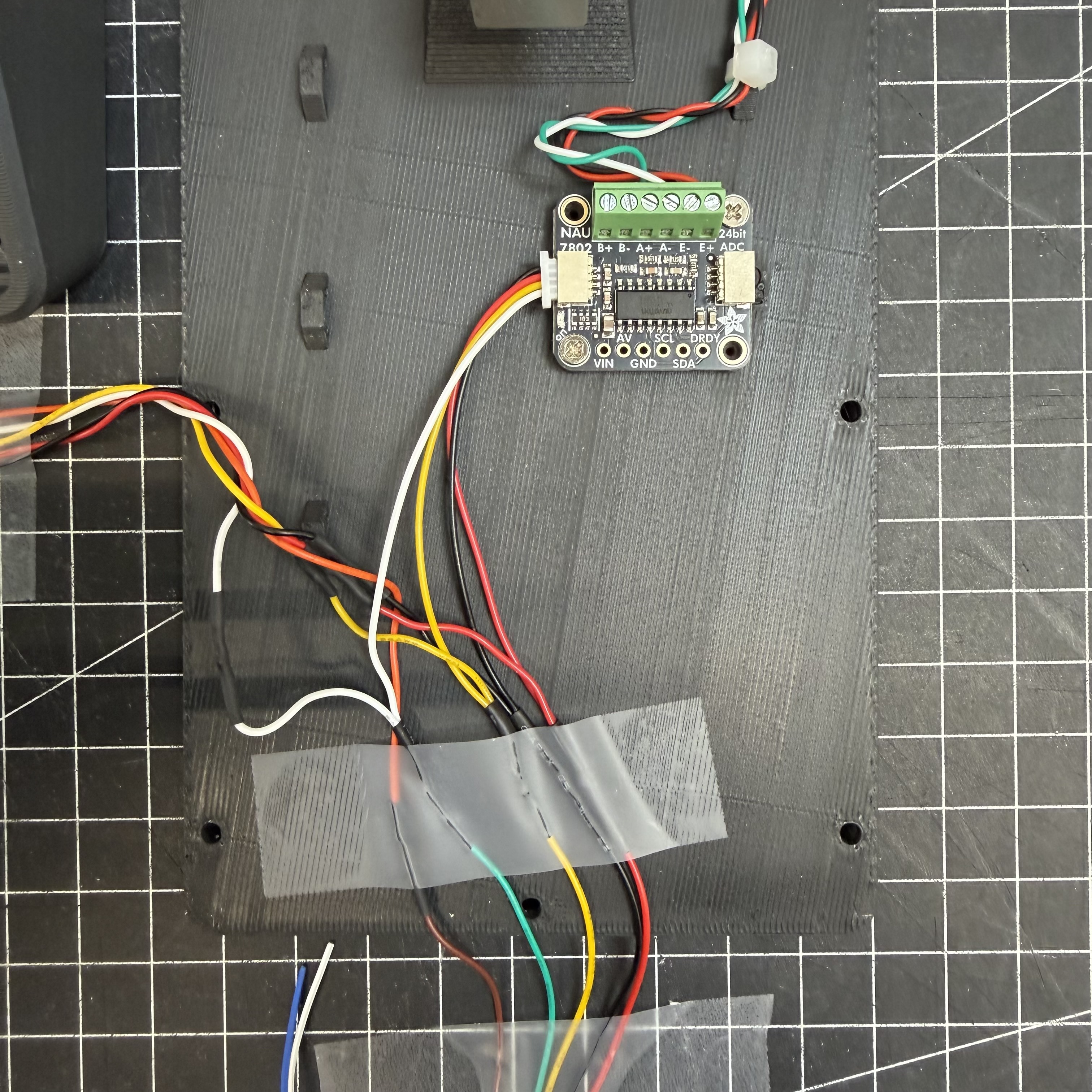
The PN532 and NAU7802 share the same I²C bus (SDA/SCL) and are wired in parallel.
Do not daisy-chain via NAU7802 STEMMA QT passthrough
The NAU7802's STEMMA QT passthrough port only supplies 3.3V. The PN532 requires 5V. Always connect both modules directly to the WT32 I/O connector.
Edit this project interactively in Cirkit Designer.
WT32-SC01 Plus I/O Connector
| Pin | Color | Signal | Connects to |
|---|---|---|---|
| 1 | Red | 5V | PN532 VCC + NAU7802 VIN |
| 2 | Black | GND | PN532 GND + NAU7802 GND |
| 3 | Yellow | GPIO10 (SDA) | PN532 SDA + NAU7802 SDA |
| 4 | Green | GPIO11 (SCL) | PN532 SCL + NAU7802 SCL |
| 5 | Blue | GPIO12 | unused |
| 6 | White | GPIO13 | unused |
| 7 | Brown | GPIO14 | PN532 RSTPDN - see the note below |
PN532 NFC Reader
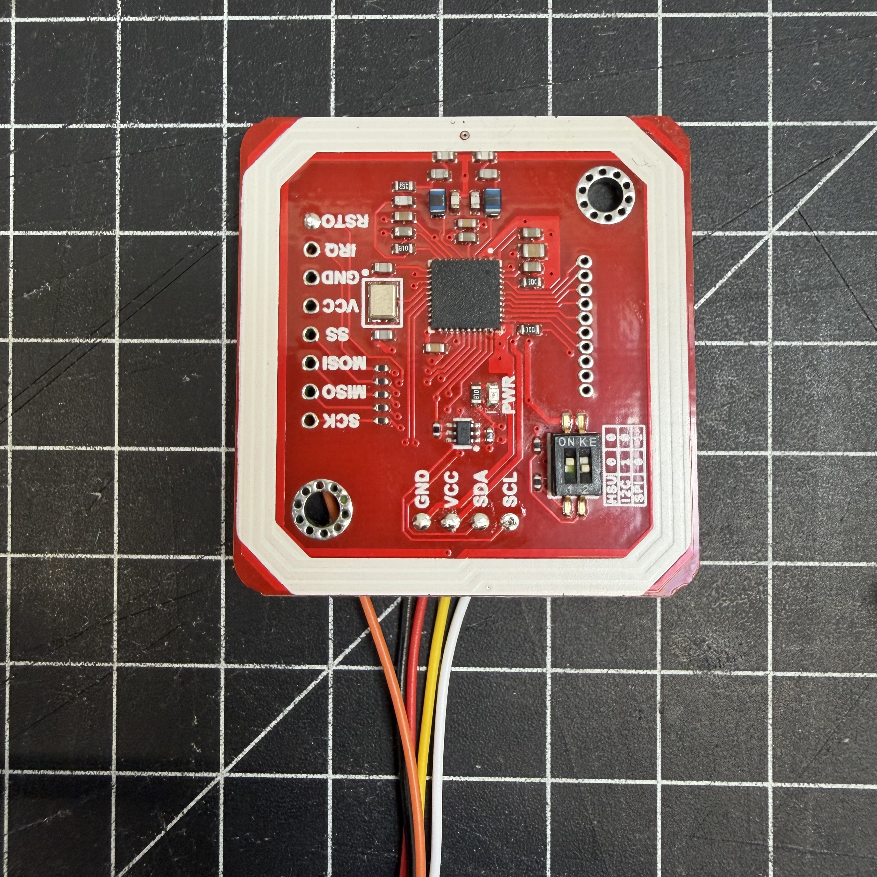
The PN532 has no connector - wires must be soldered directly.
Solder from the back
Always solder from the back of the PCB - there is not enough clearance on the front once it's mounted in the enclosure.
Recommended Assembly Order
- Solder all other components first (NAU7802, load cell, WT32 breakout cable)
- Leave the PN532 wires loose and long enough to work with
- Feed the wires up through the PN532 mount opening from below
- Solder to the back of the PN532 PCB
- Slide the PN532 into its mount and route cables into the enclosure
JST SH 1.0mm connector
If you use a 5-pin JST SH 1.0mm pigtail on the PN532, the mount opening is just large enough to pass the connector through - allowing you to solder everything outside the enclosure and plug in during final assembly.
The reset wire goes to RSTPDN
Solder the orange RST wire to RSTPDN, the pin at the end of the labelled 10-pin row (AUX1, AUX2, DBGRXD, DBGTXD, INT0, INT1, SIGCLK, SIGOUT, SIGIN, RSTPDN). With the board lying as in the photo, it is the bottom one.
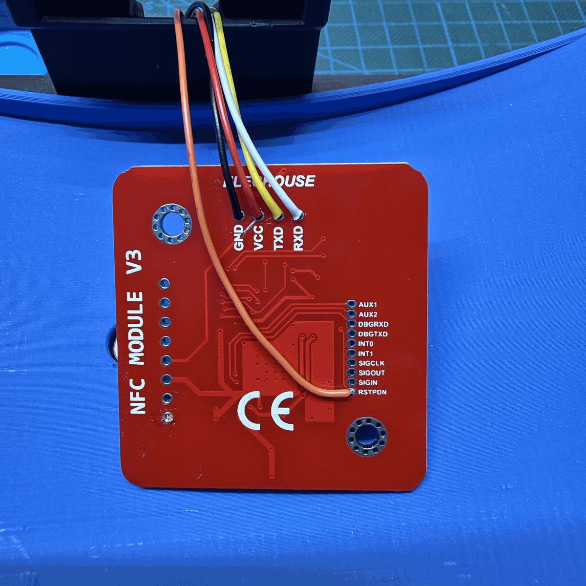
Every build guide up to August 2026 sent it to the header opposite, where the module exposes an output rather than its reset input - so the reset has never worked on any SpoolmanScale built before then.
Nothing is broken if you leave it alone. The reader has always come up fine without a reset, and a scale that is never rewired behaves exactly as it does today.
PN532 Pinout (JST SH 1.0mm 5-pin, 3rd party cable colors)
| PN532 Pin | Color (3rd party) | Signal | WT32 I/O Pin |
|---|---|---|---|
| 1 | Black | GND | Pin 2 (Black) |
| 2 | Red | 5V | Pin 1 (Red) |
| 3 | Yellow | SDA | Pin 3 (Yellow) |
| 4 | White | SCL | Pin 4 (Green) |
| 5 | Orange | RSTPDN | Pin 7 (Brown) |
After the rewiring
The scale does not take the reset line on trust. It measures it, on your device, and only uses it once the measurement says the wire is really there.
- Settings → System → Check NFC reset
- Reset line is there means the reader answered to being held in reset. The row then reads Line verified, in use, and from the next start the scale does a real hardware reset instead of only talking to the reader again.
- No effect means the wire is still on the old pad, or the joint is not making contact. Nothing changes and the scale carries on as before.
The test pulls the line to ground for five milliseconds and watches whether the reader notices. It drives open drain, so it only ever sinks - on a scale that still has the old wiring it cannot fight the module's output, which is why it is safe to offer to everyone.
What it buys you
A hardware reset is the strongest lever there is when the PN532 locks up. Without it, recovery can only talk to the reader again over I2C, which handles most cases but not all. If your reader has never stumbled, this changes nothing you will notice - which is why the scale only suggests the modification to devices where the reader has actually needed recovery.
NAU7802 Scale ADC
The safest option is soldering directly to the labeled pads on the NAU7802 (VIN, GND, SDA, SCL). Alternatively, use the STEMMA QT connector - but note that 3rd-party JST SH 1.0mm cables have a different pin order and require re-pinning.
NAU7802 Pinout (STEMMA QT, JST SH 1.0mm 4-pin)
| STEMMA QT Pin | Color (3rd party) | Signal | WT32 I/O Pin |
|---|---|---|---|
| 1 | Black | GND | Pin 2 (Black) |
| 2 | Red | 5V | Pin 1 (Red) |
| 3 | Yellow | SDA | Pin 3 (Yellow) |
| 4 | White | SCL | Pin 4 (Green) |
Load Cell
| Load Cell wire | NAU7802 terminal | Function |
|---|---|---|
| Red | E+ | Excitation + |
| Black | E- | Excitation - |
| White | A+ | Signal + |
| Green | A- | Signal - |
Negative scale values?
If the scale shows negative values, swap A+ and A-.
Full System Overview
  WT32-SC01 Plus I/O (Pins 1-7)
  ┌─────────────────────────────────────────┐
  │ Pin 1 (5V)   ───────┬─────────────────── PN532 VCC
  │                     └─────────────────── NAU7802 VIN
  │ Pin 2 (GND)  ───────┬─────────────────── PN532 GND
  │                     └─────────────────── NAU7802 GND
  │ Pin 3 (SDA)  ───────┬─────────────────── PN532 SDA
  │                     └─────────────────── NAU7802 SDA
  │ Pin 4 (SCL)  ───────┬─────────────────── PN532 SCL
  │                     └─────────────────── NAU7802 SCL
  │ Pin 7 (RST)  ─────────────────────────── PN532 RSTPDN
  └─────────────────────────────────────────┘

                                NAU7802 Screw Terminals
                                ┌──────────────────────┐
                                │ E+ ── Load Cell RED   │
                                │ E- ── Load Cell BLACK │
                                │ A+ ── Load Cell WHITE │
                                │ A- ── Load Cell GREEN │
                                └──────────────────────┘
Wiring photos